
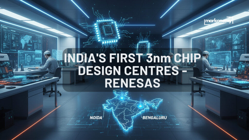
Japan’s semiconductor giant Renesas Electronics has taken a big step in strengthening India’s position in the global chip industry. The company has unveiled India’s first 3nm chip design centres in Noida (Uttar Pradesh) and Bengaluru (Karnataka).
These centres will focus on advanced semiconductor design and verification for chips as small as 3 nanometers (nm)—the latest generation of cutting-edge technology powering AI, smartphones, high-performance computing, and automotive electronics.
Renesas, a global leader in microcontrollers and analog semiconductors, said the move highlights India’s growing role as a semiconductor design hub. The two centres will employ hundreds of engineers, offering opportunities to work on world-class chip innovation.
Industry experts see this development as a milestone in India’s tech journey, especially with the government’s Semicon India initiative aiming to make the country self-reliant in chip design and manufacturing.
The opening of these 3nm design centres also brings India one step closer to joining the league of nations, driving next-gen chip technologies.
Summary Table
| Detail | Information |
|---|---|
| Company | Renesas Electronics (Japan) |
| Announcement | India’s first 3nm chip design centres |
| Locations | Noida (UP) and Bengaluru (Karnataka) |
| Focus | Advanced semiconductor design & verification |
| Technology | 3nm chips (next-gen processors) |
| Applications | AI, smartphones, HPC, automotive electronics |
| Employment | Hundreds of engineers in India |
| Alignment | Supports Semicon India initiative |
| Significance | Strengthens India’s global semiconductor role |
| Future Impact | Boosts India’s chip R&D ecosystem |